Galileo SSI I24 AI8 Anomaly Description and Image Recovery Algorithm
SSI Background
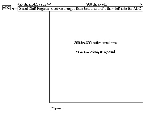
The Galileo SSI camera contains an 800-by-800 pixel CCD (charge coupled device) array for capturing images. The array pixels are coupled in the vertical direction. Along the top is an extra horizontal row of 825 elements to shift charges to the left, where they are measured by an 8-bit ADC (analog-to-digital converter). These extra 825 elements are called the "serial shift register." See Figure 1.
The serial shift register is masked off from light and serves only as a receptor for charges shifted up from the active array so they can be horizontally shifted to the left for measurement. The purpose of the extra 25 elements just before the ADC is to allow for dark pixels to be measured for automatic dark bias adjustment by a process called baseline stabilization (BLS). Whenever the active image array is shifted up by one pixel, the bottom row of pixels is ideally depleted of all charge. In the same way, whenever the top row of elements is shifted to the left, the right hand element is ideally depleted of all charge.
Prior to an image being taken, all elements are ideally depleted of charge, which happens automatically as a result of the previous image being shifted out. As light is exposed on the image array, charges build up on the individual pixels. After exposure, the process of vertically shifting the charge packets along columns of pixels and horizontally shifting the charge packets on the serial shift register begins.
For the normal 800-by-800 pixel image mode, the process is as follows:
Step 1: Shift the charge packets in the entire active image array up by one line. The charge packets from the top row of 800 pixels are now present in the 800 elements of the serial shift register above the active image array.
Step 2: Shift the charge packets in the 825-element serial shift register to the left 25 times. During this step, the ADC is nonfunctional, but the baseline stabilization (BLS) circuitry is turned on during the middle portion of this step to measure the level of "dark." This measurement is applied to an integrating circuit that forces the dark level to read about three counts on the ADC. It accomplishes this dark level adjustment with a time constant equivalent to the time required to read out about 33 rows of pixels.
Step 3: Shift the charge packets in the serial shift register to the left another 800 times, sample the measured charges with the ADC, and store them in memory.
Step 4: Repeat Steps 1 through 3 for a total of 800 times.
In anticipation of the high radiation environment during the Io close encounters, a 400-by-400 summation mode, designated AI8, was designed into the camera electronics. The radiation causes random pixels to receive extra charge, which represents added random noise in the image. By summing each group of 2-by-2 pixels, the signal-to-noise ratio is improved by a factor of 2. This camera mode was used for the majority of Io imaging on orbit 24 in October 1999. The AI8 charge-transfer process malfunctioned for these images in two different ways, referred to as anomaly 1 and anomaly 2. Most images showed only anomaly 1, but about 10% showed anomaly 2, and a few showed both anomalies in different portions of the image. The following describes the causes of anomalies 1 and 2 and a method for correcting many of the effects of anomaly 1 on the images.
Summation Mode Operation
First, a description of how the 400-by-400 summation mode was designed to work:
Step 1: Shift the charge packets in the entire active image array up by two lines. The charge packets from the top two rows of pixels are now summed in the 800 elements of the serial shift register above the image array.
Step 2: Double-shift the charge packets in the 825-element serial shift register to the left 12 times (24 total shifts) with the ADC non-functional. The BLS circuitry works as in step 2 for the 800-by-800 mode. Note that ideally there should have been 25 shifts during this step, but because of the odd number of registers and the fact that the camera circuitry is in a double shifting mode, only 24 shifts have occurred.
Step 3: Double-shift the charge packets in the serial shift register to the left another 400 times, sampling the summed charges with the ADC after each double shift and storing the measured sums in memory.
Step 4: Inhibit serial clocks for 8 clock-cycle times (equivalent to 4 double-shift times); ADC off.
Step 5: Repeat Steps 1 — 4 one more time before proceeding on to Step 6.
Step 6: Double shift the charge packets in the serial shift register to the left 7 times with the ADC non-functional.
Step 7: Repeat Steps 1 through 6 199 more times.
AI8 Anomaly 1
The AI8 summation-mode malfunction known as anomaly 1 caused single-shifting of the horizontal serial shift register instead of double-shifting. This resulted in several corruptions to the captured images.
The first and most notable corruption was an overlay of the left and right halves of the image something like a "double exposure." This also changed the aspect ratio causing the two images making up the "double exposure" to appear twice as wide as they should have.
A second corruption resulted because the automatic baseline stabilization (BLS) circuitry was misled. At the time the circuitry was expecting dark pixels, it was instead sampling a portion from the center of the image resulting in a larger amount of background subtraction to occur than it should have. Therefore, the output pixel values were much smaller than they should have been. Fortunately, since most of the measured values were twice as large as they should have been (because they were "doubly exposed"), the measured values rarely got as low as zero, below which all information would have been lost. In addition to the measured values being smaller than actual, the fact that the circuitry does not store values during the time the baseline stabilization circuitry is enabled resulted in a vertical strip of lost data down the middle of the original image. There is no way to recover this data.
A third corruption was a result of the seven extra shifts done after each pair of rows is read out of the camera (see Step 6 above). This caused the boundary at which the left and right halves of the original image were split prior to being overlaid to be shifted left and right by 7 pixels on alternating lines. This resulted in seven pixels on every other row appearing as darker "single exposed" pixels along the right hand edge of the corrupted images. It is this characteristic that fortuitously provides the mechanism to successfully de-scramble the images.
A fourth corruption was caused by incomplete flushing of the 25-element portion of the horizontal serial shift register between sampled image lines. As each line is read out, after the first 12 samples are "incorrectly" used for automatic baseline stabilization (Step 2), the next 13 samples are read out as a "single exposure" piece from near the middle of the original image (their original locations being shifted by 7 pixels on alternating lines due to the seven extra shifts between line pairs mentioned above (Step 6). This resulted in 13 darker "single exposed" pixels along the left hand edge.
The last corruption was two vertical columns of "hot" or brighter-than-normal pixels. One seen in sample 14 of even lines originates in CCD column 1 and was observed in normal 800-by-800 images. The other is seen in sample 393 of odd lines and seems to be associated with CCD column 800 but is not observed in 800-by-800 images. These defects proved to be useful features because they worked as reference points within the images to clearly indicate the exact amount of jaggedness.
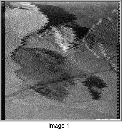
Image 1 is an example of a corrupted picture as received by the spacecraft before any corrections are applied. This image will be used during the description of the correction process to aid in understanding how the various parts of the algorithm work.
In summary, the mapping of the original image pixels on the CCD to the AI8 output images in the case of anomaly 1 is as follows:
Line 1 —
Samples 1 — 13 are from the extended pixel region of the CCD serial register and contain no valid charge
Samples 14 — 400 are the charge packets from CCD lines 1+2, columns 1 — 387 (not summed horizontally)
Line 2 and subsequent even lines —
Samples 1 — 13 are the charge packets from CCD lines 1+2, 5+6 (line 4), 9+10 (line 6), etc., columns 401 — 413 (not summed horizontally)
Samples 14 — 400 are the charge packets from CCD lines 1+2, 5+6 (line 4), 9+10 (line 6), etc., columns 414 — 800 (not summed horizontally) plus those from CCD lines 3+4, 7+8 (line 4), 11+12 (line 6), etc., columns 1 — 387 (not summed horizontally)
Line 3 and subsequent odd lines —
Samples 1 — 13 are the charge packets from CCD lines 3+4, 7+8 (line 5), 11+12 (line 7), etc., columns 408 — 420 (not summed horizontally)
Samples 14 — 393 are the charge packets from CCD lines 3+4, 7+8 (line 5), 11+12 (line 7), etc., columns 421 — 800 (not summed horizontally) plus those from CCD lines 5+6, 9+10 (line 5), 13+14 (line 7), etc., columns 1 — 380 (not summed horizontally)
Samples 394 — 400 are the charge packets from CCD lines 5+6, 9+10 (line 5), 13+14 (line 7), etc., columns 381 — 387 (not summed horizontally)
Descrambling Process
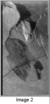
The first step in descrambling the images is to map the corrupted 400-by-400 image onto an 800-sample-by-400-line array, putting each corrupted pixel into the pixel locations from which it was summed. (We could have mapped to an 800-by-800 array, but this would only complicate the processing; instead, we wait until the array is displayed and then double the pixels in the vertical direction to restore the correct aspect ratio. Image 2 is a repeat of Image 1 with the corrected aspect ratio. Images 2 — 11 shown here have all had the pixels doubled in the vertical direction to display the correct aspect ratio.) Some pixels map to just one other pixel when they were the result of a "single exposure" (i.e., not overlain by pixels from the other half of the frame), but most of the pixels, being "double exposures," map to two pixels, one in the left-hand half of the corrected image and one in the right-hand half. Image 3 is the result of this process.
Careful analysis of the camera’s function and malfunction will reveal that the first 387 columns of this partially corrected image (approximately the left-hand half) is derived from the fourteenth through the four hundredth columns of the corrupted image. In other words, it is the corrupted image with the first thirteen columns removed. Note that almost all of this part of the image is "double exposure"--all but the top row of pixels and the last seven pixels of every other row. The next 13 columns of pixels are unrecoverable and will be displayed as a black strip down the approximate middle of the image. This accounts for the left-hand half of the corrected image.
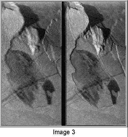
To get the right-hand half of the partially corrected image, we first have to eliminate the top row of the corrupted image and provide a blank row at the bottom. Then we have to offset every even-numbered row by seven pixels to the right (providing seven blank or black pixels on the left). This constitutes the right-hand half of the partially corrected image. Note that in the left-hand half the entire top row is "single exposure" but in the right half it is not present. Note also that the "single exposure" pieces along the right-hand edge are also not present on the right. The only place where there are "single-exposure" pixels in the right-hand half of the partially corrected image is along its left edge (near the center of the full image). These "singly exposed" rows alternate with missing data for samples 401 - 407, are contiguous for samples 408 - 413, and alternate with "double exposure" rows for samples 414 - 420.
Displaying the images in this way allows some of them to show improvement, particularly those that have details in the left and right halves of the image that don't overlap. Any detail that belongs in the left half of the image will display 7-pixel-wide, jagged contrast boundaries in the right half of the image, and any detail that appears jagged in the left half of the image (and also in the corrupted image) will appear unjagged in the right half of the image where it properly belongs, since every other line has been offset by seven pixels.
The next step in descrambling is to observe that if we knew the true intensity of either contributor to the "double-exposure" pixels in the partially corrected images, we would also know the true value of the sister pixel with which it was combined from the other half of the image by simply subtracting the true value from the "double-exposure" value. We also assume that if we know the true values of the pixels above and below an unknown pixel, we can approximate the unknown pixel as simply the average of the two known pixels adjacent to it.
If we look along the right-hand edge of the left half of the partially corrected image, we will see that the pixels alternate between "single-" and "double-exposure" as we go down. We can correct this seven-pixel wide column by averaging the pixels above and below the "double-exposure" pixels to approximate the true value of the pixel in the "double-exposed" line. Then we subtract the averages from the "double-exposure" values and replace the sisters on the right half of the image.
After going down the entire seven-pixel wide column, we observe that now the right-hand edge of the right half of the image has an alternating pattern of "single-" and "double-exposure" pixels. We can replicate a similar process of calculating averages down the right hand edge of the image, subtracting from "double-exposure" values, and replacing sisters in the left half of the image.
This will result in another set of alternating "single-" and "double-exposure" pixels on a new column seven pixels to the left of the original one, and we can repeat this process until the entire image has been corrected.
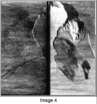
Image 4 is the result of applying this correction. Note that although the two halves of the image vary greatly in intensity and there is a lot of noise introduced, the separation of the features into their appropriate halves (as determined by their jagged edges in Image 3) is quite accurate.
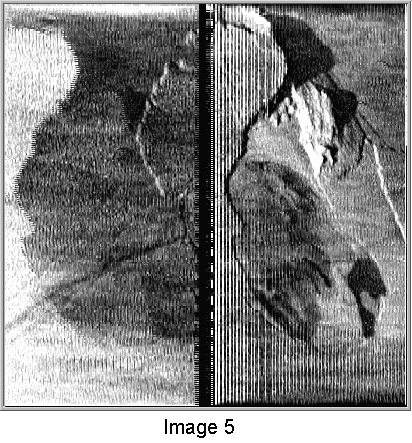
Instead of doing all of the above, we could have started near the left-hand edge of the right half of the partially corrected image and worked our way to the right, correcting both halves until the entire image was corrected. Image 5 is the result of this process. Note that in addition to similar intensity variations and noise exhibited in Image 4, there is a severe "shadow" of a feature from the right half of the image showing up in the left half and that there are vertical stripes in the right half of the image.
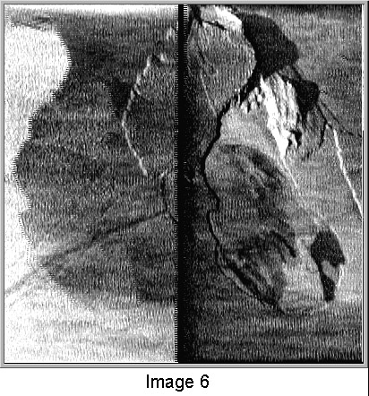
The vertical stripes are caused by the "hot" pixels present in the original image near the left and right edges. We provide options for overwriting particular columns (or samples) of pixels with adjacent columns. Image 6 is the result of overwriting column 13 with column 12 prior to descrambling. Note that this completely eliminates the coherent vertical striping although there remains incoherent (or jittery) striping.
We can also copy columns near the right edge of the image to eliminate the hot pixels near the right edge of both halves of the image, although in this case, these hot pixels don’t cause vertical striping throughout the image.
The foregoing is the major contribution to the correction process. It was initially expected that this process would work well at the start but that errors would accumulate making the image look worse or unacceptable towards the end of the process, but instead the process tends to converge on the same final result even if the original "true" values for the "single-exposure" pixels are off by a significant amount.
As it turns out, the original "true" values are off by a significant amount due to the baseline stabilization (BLS) circuitry. Close examination of the "single-exposure" pixels will reveal that near the top of the image, they actually contain detail, but after a few dozen rows down, most of them turn quite dark. To correct for this, we simply add an offset with a "time-constant," i.e., we add zero to all the pixels on the first row and increasingly larger values to successive rows in an exponential manner approaching an arbitrary limit, which we can adjust to get the best corrected image. If this bias adjustment value is too large or too small, the two processes of correction (center-to-right and center-to-left) will be significantly different. To find the correct bias value, the operator observes the individual corrections and finds a value that minimizes the difference between them. This offset is added before the corrections described earlier are applied.
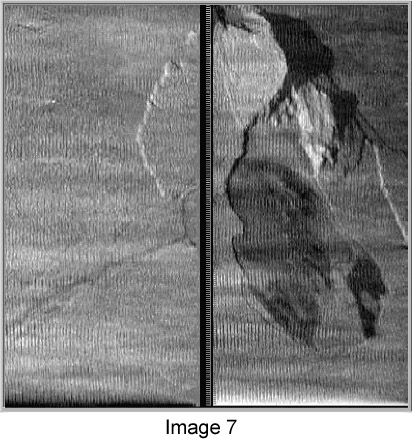
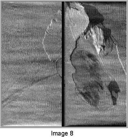
Images 7 and 8 have an offset of 40 applied to them. Image 7 is the bias-adjusted version of the center-to-left correction shown in Image 4, and Image 8 is the bias-adjusted version of the center-to-right correction shown in Image 6. Note how the intensity variations between the left and right halves of the image and the shadow in Image 6 are completely eliminated. In fact, the two processes produce almost identical results. The major difference between them is the dark and light streaking along the top and bottom edges caused by the inability of the algorithm to properly average pixels above and below, since there is nothing above or below with which to average.
However, the next step is to average the two images together, which partially corrects for the streaking at the top and bottom of the image and reduces other intensity variations in the corrected image. Image 9 is the result of this averaging.

The correction algorithm run this far produces a lot of vertical stripes at approximately seven-pixel offsets. To get rid of these, we incorporate a special "notch" filter that removes these stripes. It is special because it works jointly between sister pixels and conserves the total signal. It works as follows. First a two-dimensional array is built that corresponds to the difference between sister pixels. Then this array is scanned and from each difference element, the average of the seven elements starting three elements to the left and including the three elements to the right is subtracted. Half of this difference is subtracted from the source sister pixel from the left half of the image and added to the source sister pixel from the right half of the image. The filter is not applied to the three columns along the left and right-hand edges of the image that include the sister pixels. Image 10 is the result of this notch filter.

Unfortunately, this filter works a little too well and removes some of the detail and introduces slight ghosts or shadows from the other half of the image. To counteract this, we apply another special signal-conserving filter that also works with sister pixels to add back some of the detail. It works in a similar way by creating a two-dimensional array corresponding to the new difference between sister pixels. Then a weighted average is calculated on the same seven elements starting three to the left and extending three to the right of each element. The weighting factors are: one for the two pairs of outside elements, negative one for the next two inside elements and negative two for the center element, all divided by six. These factors were derived empirically. The weighted average is subtracted from the source sister pixel from the left half of the image and added to the source sister pixel from the right half of the image. Again, the filter is not applied to the three columns along the left and right-hand edges of the image that include the sister pixels. Image 11 is the result of this filter and represents the final product. You have to look very closely to see the improvement between Images 10 and 11.
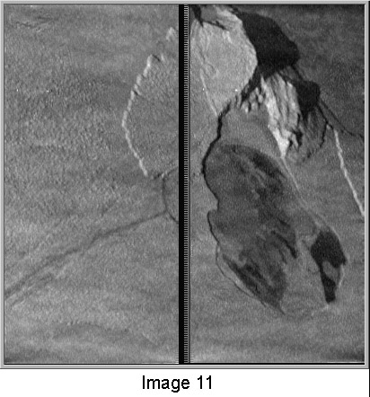
Overall, the total algorithm produces excellent results except at the top and bottom edges of the image where the averaging of pixels above and below don't apply. It also has problems with high contrast details that follow an almost horizontal path where the averaging doesn't work properly. Another source of error is where there is a pattern that has a seven-pixel-wide repeat that gets partially filtered out. All of these errors are obvious by looking at the final image because they produce darkness in one half and corresponding lightness in the other half, or a ghost in one half of an object in the other half. In the left half of Image 11, there is a faint ghost from the top of the dark flat area below the two raised peaks and another ghost from the notch in the upper raised structure.
Some of the I24 images exhibiting AI8 anomaly 1 also include what looks like horizontal streaking of the image data in some bright areas. In these cases, the full-well capacity of the serial register was exceeded in these areas as a result of the "double exposure" line summing that occurred. The full-well capacity of the serial register pixels is larger than that of pixels in the 800x800 array by a factor of at least 2 (this allows the vertical summing of the 2x2 summation to take place in the serial register; the horizontal summing does not occur until the charge packets reach a final summing well at the output end of the serial register). However, the I24 AI8 anomaly 1 images (all of which were taken using gain state 1) that were exposed to the higher end of the encoding range produce charge levels that exceed the serial register full-well capacity. Refer to Section III.D.2 and Figure 3-34 of the pre-launch SSI Calibration Report, Part 1, (available on CD-ROM Vol. GO_0001) for discussion and an example of images exceeding full-well in the array columns, resulting in vertical "smearing." The I24 AI8 anomaly 1 streaking is the same phenomenon but in the horizontal direction.
A set of 14 I24 images that exhibit this anomaly to at least some degree have been identified. In some, the effect is very minor; in others, nearly the entire frame is washed out. The variation in the zero-signal DN level due to the Baseline Stabilization (BLS) sampling non-zero-charge pixels (because of the other readout anomalies) makes determining the actual original signal level within the CCD in electrons fairly uncertain. However, a best estimate shows that the serial register full-well level was exceeded at output signal levels equivalent to about 190 gain-state-1 DN or about 300,000 electrons. The list of images exhibiting serial full-well limitations is:
| SCLK | PICNO | Estimated BLS zero point (DN) |
Maximum output DN |
Actual maximum (DN) |
Notes |
| 520793266 | 30 | -70 | 155 | 225 | Some possible smearing in bright patches |
| 520793270 | 31 | -70 | 125 | 195 | Some possible smearing in bright patches |
| 520793273 | 32 | -70 | 135 | 205 | Some possible smearing in bright patches |
| 520793284 | 35 | -70 | 125 | 195 | Maybe one very small smeared bright patch |
| 520794087 | 58 | -90 | 105 | 195 | Most of right side smeared |
| 520795742 | 75 | -100 | 100 | 200 | Smearing in large areas on right side |
| 520795745 | 76 | -110 | 80 | 190 | Smearing in large areas on right side |
| 520795880 | 78 | -85 | 110 | 195 | Large smear on right and bottom |
| 520795884 | 79 | -170 | 60 | 230 | Almost entirely smeared |
| 520797287 | 91 | -80 | 105 | 185 | Smear on lower right third |
| 520797307 | 94 | -80 | 100 | 180 | Smear in bright area on right center |
| 520797310 | 95 | -70 | 110 | 180 | Maybe a small area on the right |
| 520797445 | 97 | -75 | 110 | 185 | Some small bright areas smeared on right |
| 520797449 | 98 | -90 | 100 | 190 | Large areas on right side and bottom |
The full well seems to trend toward a lower level for the right side of the output frame than for the left. This is what would be expected since charge is transferred from right to left in the serial register during readout, and the full-well limit for any column will be the lowest full-well encountered by its charge packet during serial readout. What is really seen is full well trending lower from left to right over columns 1 to about 400 in the actual serial register. Columns above about 400 in the serial register never see more than 2 pixels of charge from the CCD array for anomaly 1 because horizontal summing does not take place until the end of the serial transfer; thus, charge packets traversing the serial register above about sample 400 contain at most about 160,000 electrons. However, because of the incomplete serial transfer of each line in anomaly 1 and the consequent adding of two line pairs (left half of one line pair added to the right half of the previous line pair) in samples 1 to about 400 of the serial register, those serial register pixels see 4 pixels worth of charge or up to 320,000 electrons - higher than the full-well level.
No correction for the horizontal streaking is possible.
AI8 Anomaly 2
AI8 anomaly 2 is characterized by a "vertical bars" pattern in the I24 AI8 images. See Image 12. What appears to be happening in those regions of the images containing vertical bars is that horizontal summation (i.e., two serial shifts per ADC sample period) is successfully occurring only half the time. In the brighter bars, we have 8 samples that were correctly summed in the horizontal direction, while in the darker bars, we have 8 samples that are full horizontal resolution (i.e., horizontal summing did not occur as in AI8 anomaly 1). For every 32 serial clock cycles, we are getting only 24 actual serial charge packet transfers (16 to create the first 8 summed pixels followed by 16 that result in only 1 transfer per ADC sample period to create the next 8 unsummed pixels). Incomplete shifting of the CCD serial register during the course of a line time results in the next parallel transfer overwriting the last ~180 columns of data from the previous line. These overwritten data are then clocked out during the next line time and show up in image samples 1 — 123. We thus have four different types of image samples: (1) the bright bars below sample 123 consist of charge summed from 8 CCD pixels (4 rows, 2 columns each), (2) the darkbars below sample 123 consist of charge summed from 4 CCD pixels (4 rows, 1 column each), (3) the bright bars above sample 123 consist of charge summed from 4 CCD pixels (2 rows, 2 columns each), and (4) the darkbars above sample 123 consist of charge summed from 2 CCD pixels (2 rows, 1 column each). The transition line(s) between anomalies 1 and 2, when they occur in the same frame, has not been analyzed in detail.
The mapping from CCD array row/column to output image line/sample for anomaly 2 is as follows [note: the sums inside parentheses below represent column numbers, not the sum of DN values from two different columns]:

Line 1 —
Samples 1 — 4, extended serial register pixels with no valid charge
Samples (16n+5) thru (16n+12), CCD rows 1+2, columns (24n+0)+(24n+1), (24n+2)+(24n+3), …(24n+14)+(24n+15), for n = 0, 24
Samples (16n+13) thru (16n+20), CCD rows 1+2, columns (24n+16), (24n+17), …(24n+23), for n = 0, 23 [no column summation]
Samples 397 — 400, CCD rows 1+2, columns 592 — 595 [no column summation]
Line 2 and subsequent even lines —
Samples 1 — 4, CCD rows 1+2, columns 616 — 619 [no column summation]
Samples (16n+5) thru (16n+12), CCD rows 1+2, columns (24n+620)+(24n+621), (24n+622)+(24n+623), …(24n+634)+(24n+635) plus CCD rows 3+4, columns (24n+0)+(24n+1), (24n+2)+(24n+3), …(24n+14)+(24n+15), for n = 0, 6
Samples (16n+13) thru (16n+20), CCD rows 1+2, columns (24n+636), (24n+637), …(24n+643) plus CCD rows 3+4, columns (24n+16), (24n+17), …(24n+23), for n = 0, 6 [no column summation]
Samples 117 — 122, CCD rows 1+2, columns 788+789, 790+791,…,798+799 plus CCD rows 3+4, columns 168+169, 170+171,…,178+179
Sample 123, CCD rows 1+2, column 800 plus CCD rows 3+4, columns 180+181
Sample 124, CCD rows 3+4, columns 182+183
Samples (16n+13) thru (16n+20), CCD rows 3+4, columns (24n+16), (24n+17), …(24n+23), for n = 7, 23 [no column summation]
Samples (16n+5) thru (16n+12), CCD rows 3+4, columns (24n+0)+(24n+1), (24n+2)+(24n+3), …(24n+14)+(24n+15), for n = 8, 24
Samples 397 — 400, CCD rows 3+4, columns 592 — 595 [no column summation]
Line 3 and subsequent odd lines —
Samples 1 — 4, CCD rows 3+4, columns 623 — 626 [no column summation]
Samples (16n+5) thru (16n+12), CCD rows 3+4, columns (24n+627)+(24n+628), (24n+629)+(24n+630), …(24n+641)+(24n+6421) plus CCD rows 5+6, columns (24n+0)+(24n+1), (24n+2)+(24n+3), …(24n+14)+(24n+15), for n = 0, 6
Samples (16n+13) thru (16n+20), CCD rows 3+4, columns (24n+643), (24n+644),…(24n+650) plus CCD rows 5+6, columns (24n+16), (24n+17), …(24n+23), for n = 0, 6 [no column summation]
Samples 117 — 119, CCD rows 3+4, columns 795+796, 797+798, and 799+800 plus CCD rows 5+6, columns 168+169, 170+171, and 172+173
Samples 120 - 124, CCD rows 5+6, columns 174+175, 176+177,…, 182+183
Samples (16n+13) thru (16n+20), CCD rows 5+6, columns (24n+16), (24n+17), …(24n+23), for n = 7, 23 [no column summation]
Samples (16n+5) thru (16n+12), CCD rows 5+6, columns (24n+0)+(24n+1), (24n+2)+(24n+3), …(24n+14)+(24n+15), for n = 8, 24
Samples 397 — 400, CCD rows 3+4, columns 592 — 595 [no column summation]
This model matches all the primary features of the AI8 images that include anomaly 2. It predicts the positions and widths of the vertical bars. It predicts the 2x difference in signal level between adjacent bright and dark bars. It predicts the position of the end of the overlap region between the right side of a line and the left side of the next line. It predicts the odd/even line offset in the overlap region below sample 123. It predicts the location of the dead pixel found at CCD row 384, column 178 (found at line 192, sample 121). It predicts the change in slope of the limb of Io between the bright and dark bars in PICNO 84 (SCLK 520797135).
On average, the signals in the output image pixels that came from summing two 1-column x 2-row blocks from different columns [type (2) described above] have a higher DN level than pixels that come from 2x2 blocks of adjacent pixels [type (3)] even though both contain 4 pixels worth of charge electrons. This suggests that when two serial shifts do not occur in an ADC sampling period, it is because the second clock pulse in the sampling period does not effectively transfer charge. This conclusion derives from the fact that the ADC samples an exponentially rising voltage whose amplitude is proportional to the number of charge electrons transferred during each pixel period. If horizontal summation is happening correctly [as for type (3) pixels], two exponential voltage swings are added together, one delayed slightly from the first, before the ADC sample is taken. This is what causes the ~25% increase in gain for the summation mode relative to non-summation modes. When only a single exponential waveform is generated with the same amplitude (same total electron charge) as the sum of the two having half the amplitude (charge), it must originate earlier than the second pulse in correct summation relative to the ADC sample time in order to yield a higher DN value. Therefore, since only one serial clock pulse is effective for type (2) pixels, it must be the earlier pulse of the two normally issued per sampling period in the summation mode.
Also note that the baseline stabilization (BLS) circuit, which is supposed to keep the zero-exposure level at a small positive DN value, is being misled by the incomplete clocking of the serial register. Rather than sampling the zero level in the extended pixel region of an empty serial register, it samples the extended pixel region while it still has charge in it from the CCD array. To first order, the BLS samples a mixture of 2x2 and 1x2 summed signals from the array. It then tries to drive the average of these values, which is roughly 3/4 of the average signal on the right side of the frame, to low DN. This occurs over a period of about 50 line times given the BLS time constant. So we see the output DN level ramping down exponentially over the first 50 or so lines. Below that, the zero level has been adjusted so that 2x2- and 1x4-summed regions end up at about 1/4 of their true value, and 1x2-summed areas go negative and show up as 0 DN. 2x4-summed areas end up at about 5/8 of their true value.
Although the spatial pattern of the anomaly 2 vertical bars is identical to that of the bars seen in HIS-mode images in C22, what is generating the output DN variations is not the same. The signal difference between adjacent HIS bright and dark bars is a fixed gain-dependent delta, not a factor of 2x. The HIS images show no evidence that all the serial charge transfers are not taking place properly — there are no discontinuities in the underlying scene patterns and no boundaries indicative of parallel transfers occurring before the serial register is completely emptied. However, the similarity in the spatial patterns of the HIS and AI8 bars indicates that the root cause of both is very likely the same (and the same as that of AI8 anomaly 1, too), originates within the SSI, is most probably radiation dose or dose rate dependent, has a binary characteristic synchronized with the SSI master clock, and involves the CCD serial clocks and/or the initial stages of the CCD signal chain.
The horizontal streaking in bright image areas is only apparent in conjunction with anomaly 1. When an image exhibits anomaly 2, the serial full-well limit is never clearly evident. That may be because for anomaly 2, the high signal areas where two line pairs have been added together in the serial register is confined to samples left of about 183 where the serial full well appears to be higher.
A correction algorithm for anomaly 2 has not yet been developed.